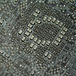
No electronics manufacturing process can take place without proper PCB inspection. A faulty PCB can cause a wide range of problems in the electronic device where it is used. It can be more expensive for the product manufacturer to recall the products if even one component of the PCB fails to operate as expected. An early detection of faults in the PCB helps avoid such problems. The inspection of PCB is a complex process. It involves visual, manual and automatic inspections. Advanced imaging and x-ray machines are needed to inspect the soldering joints and copper etchings.
The Manual Inspection
It is simply a visual inspection process that is performed manually by a technician. Obvious problems can be detected with this inspection method. It is a costly approach to inspect the PCBs and provides poor results. Manual inspection was the only method to inspect PCBs in earlier times. It is no longer performed due to availability of automatic and more advanced inspection systems that deliver highly accurate results.
Automatic Optical PCB Inspection
Now it is the most widely used method for inspecting the PCBs. The inspection machine has an optical system to take images. In this inspection process, the first step is to take an image of a well made PCB with accurate component placements. In the next steps, images of other PCBs are taken and compared to this first image. Any variation in the image helps detect the fault quickly. Many issues can be detected with the help of automated optical inspection. It has been perfected over the years and become the most reliable PCB inspection option.
X-Ray Inspection
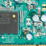
With increasing density of components placed on the PCBs, it has become difficult to correctly verify a PCB using only visual, manual or optical inspection methods. An x-ray machine designed specifically for inspecting PCBs is now used to inspect PCBs with dense component placements. Due to its x-ray technology, the equipment can look under the chips and components. While it is an expensive inspection method, it delivers highly accurate result for the small form factor SMT PCBs.
The main purpose of any PCB inspection process is to identify the defects before the PCB moves ahead in the manufacturing process of a device. Some defects may be going on from the start while others may start appearing after production of certain number of PCBs. This is the reason each PCB requires proper inspection before being used in the final product. PCB defects corrected in time help avoid costly rejects and product recalls. It is an important part of the PCB fabrication process.